
AMD Supercharges AI Knowledge Facilities With Highly effective MI350 GPU At Advancing AI 2025

Take a look at our newest merchandise
![[Netflix Certified & Auto Focus] Smart 4K Projector, VGKE 900 ANSI Full HD 1080p WiFi 6 Bluetooth Projector with Dolby Audio, Fully Sealed Dust-Proof/Low Noise/Outdoor/Home/Bedroom](https://i0.wp.com/m.media-amazon.com/images/I/71yY+2ryOZL._AC_SL1500_.jpg?w=300&resize=300,300&ssl=1)
![[Netflix Official & Auto Focus/Keystone] Smart Projector 4K Support, VOPLLS 25000L Native 1080P WiFi 6 Bluetooth Outdoor Projector, 50% Zoom Home Theater Movie Projectors for Bedroom/iOS/Android/PPT](https://i2.wp.com/m.media-amazon.com/images/I/71Emwd78tlL._AC_SL1500_.jpg?w=300&resize=300,300&ssl=1)


AMD Debuts Its Subsequent Gen Al MI350 Accelerator And Full-Stack, Rack-Scale AI Platforms
On the Advancing AI occasion, at the moment underway in San Jose, California, CEO Dr. Lisa Su, together with an array of firm execs and companions, disclosed AMD’s newest built-in AI platform imaginative and prescient and unveiled new rack-scale AI methods, in further to particulars relating to its forthcoming Intuition MI350 collection AI accelerators, Pensando Pollara 400 AI NICs, and the ROCm 7 software program stack.
A myriad of AMD’s companions, from Meta, to Microsoft, and Oracle additionally mentioned their profitable Intuition MI300 collection deployments and expressed commitments to future merchandise, just like the MI350, and the next-generation MI400 collection and AI rack codenamed “Helios”.
AMD Intuition MI350 Sequence Particulars
The AMD Intuition MI350 collection will encompass the MI350X and MI355X. Each of those AI accelerators are basically comparable and have the identical silicon and options set, however the MI350X targets decrease energy air-cooled methods, whereas the MI355X targets denser liquid-cooled configurations. As such, the chips function at totally different frequencies and energy ranges, which can finally have an effect on efficiency, however we’ll get to that in only a bit.
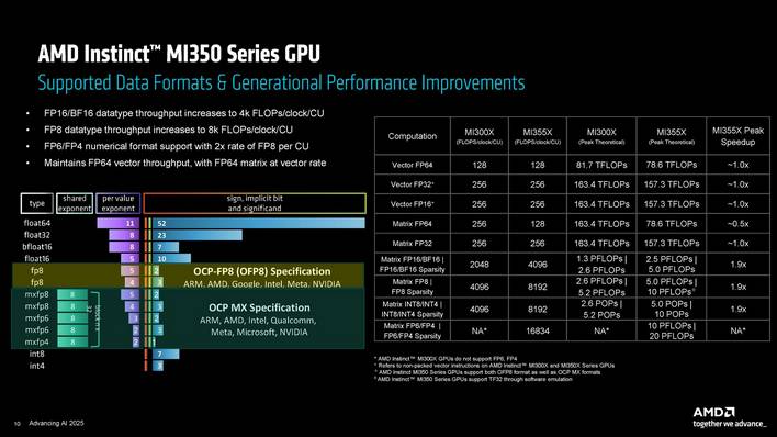
We’ve disclosed some preliminary particulars relating to the MI350 collection (the MI355X specifically) previously however have further info to share right now. To rapidly recap our earlier protection, the MI350 collection compute dies are manufactured utilizing a extra superior 3nm course of node in comparison with the MI300 collection, the accelerators characteristic 288GB of sooner HBM3e reminiscence, and so they help new FP4 and FP6 knowledge sorts. The MI350 collection additionally leverages the newer CDNA 4 structure, which is healthier suited to right now’s extra various AI and ML-related workloads.
The CDNA 4-based Intuition MI350 collection options enhanced matrix engines, with help for brand new knowledge codecs and blended precision arithmetic. The multi-chiplet SoCs additionally characteristic Infinity Material and package deal connectivity enhancements, all of which culminate in improved efficiency and vitality effectivity. Extra particularly, adjustments to the compute engines, reminiscence configuration, and to the SoC structure optimize reminiscence utilization and vitality use, which in flip preserve the cores higher fed to optimize utilization, general efficiency and effectivity. All instructed, AMD claims its staff has doubled the throughput with the MI350 collection versus the earlier gen with lower than double the ability. AMD additionally lowered the uncore energy within the design, which affords further energy for the compute engines, once more for larger efficiency.
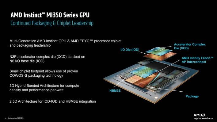
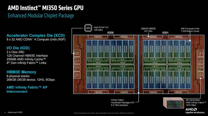
By way of their precise configuration, MI350 collection SoCs are constructed utilizing eight XCDs, or Accelerator Complicated Dies, which sit atop twin IO dies which are located within the center layer within the 3D stack. A CoWoS interposer homes the IO dies and HBM stacks, and the compute chiplet stacks are 3D hybrid bonded on prime of the IO dies. As beforehand talked about, the XCDs are manufactured on TSMC’s superior 3nm course of (N3P), however the IO dies are manufactured utilizing a 6nm course of.
Every of the eight XCD options 32 CDNA 4-based Compute Models, for a grand complete of 256 CUs and 1,024 matrix engines. And the IO dies characteristic a 128 channel HBM3e interface, 256MB of Infinity Cache, and a complete of seven 4th Era Infinity Material hyperlinks providing 1,075GB/s of peak bandwidth. An Infinity Material AP (Superior Packing) hyperlink connects the 2 IO collectively and provides a large 5.5TB/s of bidirectional bandwidth.
Together with the XCDs and IO dies, there are eight bodily stacks of HBM3e reminiscence, 36GB per stack (12-Hello), for a complete capability of 288GB. The reminiscence operates at 8Gbps, which ends up in 8.0TB/s of peak bandwidth.
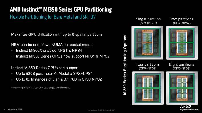
AMD additionally made adjustments to the methods the GPUs and reminiscence might be partitioned. The MI350 collection GPUs might be cut up into as much as 8 spatial partitions and the HBM can function in one in all two NUMA per socket modes – NPS1 or NPS2. The MI300 collection supported NPS1 or NPS4 reminiscence configurations.
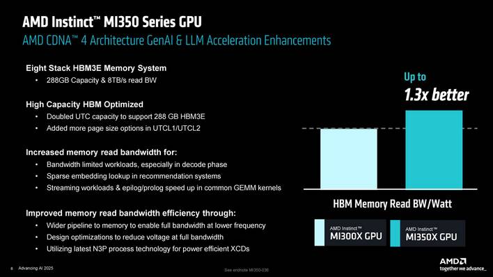
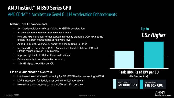
There are additionally energy advantages to utilizing HBM3e. HBM3e provides as much as 1.3x higher reminiscence learn bandwidth per watt versus the earlier gen and the structure provides 1.5x larger peak HBM learn bandwidth per CU. As a result of larger bandwidth general, and the less complete compute models versus the MI325X (304 CUs vs 256), extra bandwidth is on the market per CU, which helps for workloads which are bandwidth certain.
AMD Intuition MI350 Based mostly Rack Degree Options
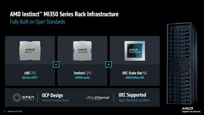
The apparent aim for AMD is to promote as many MI350 collection accelerators as doable, supported by different AMD silicon. To that finish, the corporate additionally launched new rack scale options that leverage AMD EPYC processors and AMD Pensando community expertise, together with the MI350 collection.
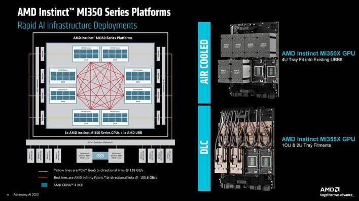
There are two fundamental rack scale options coming down the pipeline, the MI355X DLC and MI350X AC. The MI355X is the Dense Liquid Cooled answer, whereas the MI350X is the air-cooled possibility.
The MI355X DLC can pack as much as 128 MI35X accelerators, in 8 2U chassis, racked 16 excessive. The MI350X AC packs 8 MI350X accelerators into every 4U chassis, for a complete of 64 per rack.
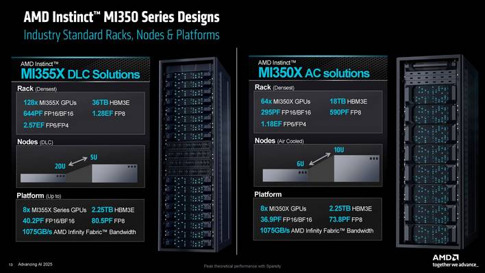
The MI355X DLC operates at 1.4kW, whereas the MI350X operates at 1kW. To attain that discount in energy, the MI350X’s compute models run at about 10% decrease clocks, that are mirrored within the theoretical peak efficiency numbers within the slide. We’re instructed, nonetheless, that the real-world efficiency distinction will doubtless be about 20% relying on the actual workload.
AMD Pensando Networking Expertise Updates
Quick and dependable community connectivity is paramount in right now’s AI knowledge facilities. The front-end shuttles knowledge to an AI cluster, and the backend handles knowledge transfers between compute nodes and clusters. If both the entrance or backend are bottlenecked, the compute engines and accelerators within the system aren’t optimally fed knowledge, which ends up in decrease utilization and probably misplaced income or diminished high quality of service.
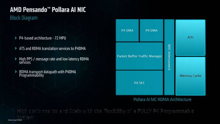
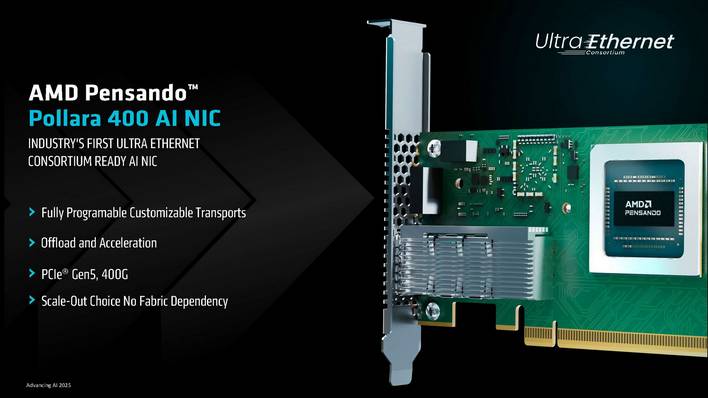
To speed up and handle the entrance and backend networks, and offload the CPUs in a system, AMD provides Pensando Salina DPUs for the front-end and the Pensando Pollara 400 AI Community Interface Card, the business’s first Extremely Ethernet Consortium (UEC) prepared AI NIC, for the again finish.
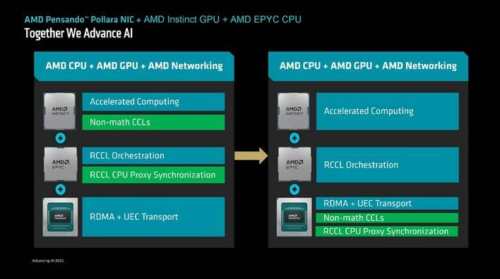
The AMD Pensando Pollara 400 AI NIC, which is now transport, is powered by the AMD P4 Programmable engine. The AMD Pensando Pollara 400 helps the most recent RDMA software program and provides quite a few new options to optimize and improve the reliability and scalability of high-speed networks.
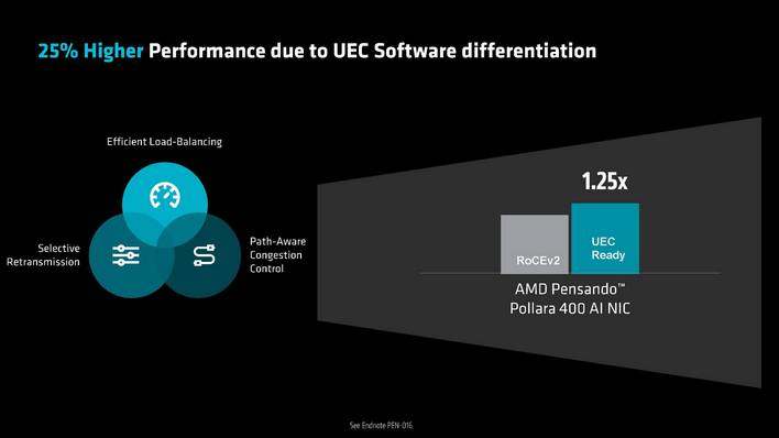
For instance, the Pensando Pollara 400 helps path conscious congestion management, to extra effectively route community site visitors. It additionally helps quick misplaced packet restoration, which may extra rapidly detect misplaced packets and resent simply that single packet to optimize bandwidth utilization. And it helps quick community failure restoration as effectively.
AMD Updates Its ROCm Open-Supply Software program Stack
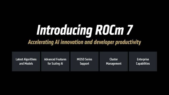
Along with displaying off its newest {hardware} applied sciences, AMD made some large bulletins relating to its ROCm software program stack. For the uninitiated, ROCm is AMD’s software program stack, which incorporates drivers, improvement instruments, and APIs for programming the corporate’s GPUs.
Together with introducing ROCm 7, AMD stated it’s re-doubling its efforts to raised join with builders and launched the AMD Developer Cloud and Developer Credit.
ROCm 7 expands help for extra AMD GPUs, particularly on the shopper, absolutely helps each Linux and Home windows, and incorporates all the optimizations and efficiency enhancements launched over the lifetime of the ROCm 6.
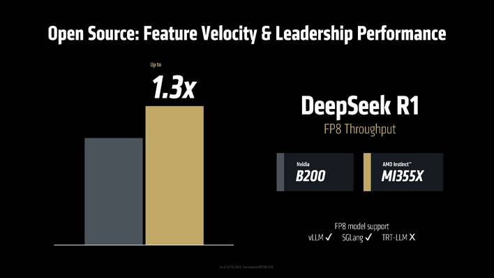
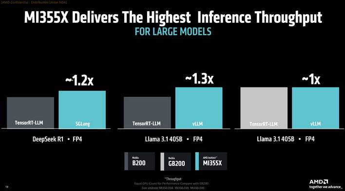
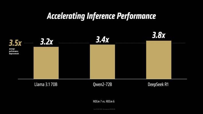
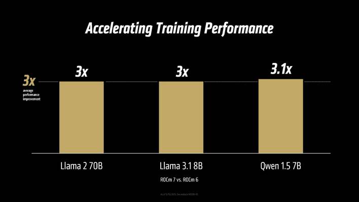
Model 7 provides roughly 3X the coaching efficiency over ROCm 6 and the open-source nature of the software program affords sooner optimization for rising fashions. To that finish, it confirmed the MI355X’s FP8 throughput with DeepSeek R1 outpacing the NVIDIA B200 by as much as 30%.
AMD Wanting To The Future
AMD isn’t standing nonetheless, after all. Dr. Su additionally revealed some new particulars relating to the following gen MI400 collection, Zen 6 based mostly EPYC “Venice” CPUs, and Pensando NICs codenamed “Vulcano”.
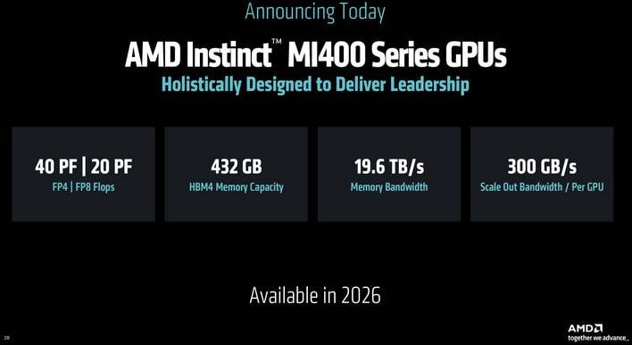
The MI400 can be based mostly on a completely new structure, help new knowledge sorts, and supply large will increase in bandwidth and compute. AMD is claiming as much as 40PF and 20PF of FP4 and FP8 compute, respectively, an enormous 432GB of HBM4 providing a whopping 19.6TB/s of peak bandwidth, and 300GB/s of scale out bandwidth.
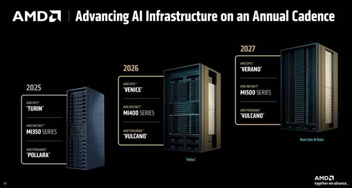
We’ll have to attend some time for extra particulars relating to MI400, Zen 6, and the Pensando “Vulcano” AI NIC, however relaxation assured, they’ll supply extra compute, extra bandwidth, the most recent IO, and future software program improvements assist tie all of it collectively.
AMD made a large number of daring claims at its newest Advancing AI occasion and revealed fairly a bit about its future plans and imaginative and prescient. Like NVIDIA, AMD’s not simply making chips. The corporate now provides AI options spanning low-power shoppers all the best way as much as the rack degree, and it’ll clearly broaden its choices shifting ahead. We suspect most of AMD’s disclosures this yr can be well-received and look ahead to what the corporate has in retailer for subsequent yr.
![[Win 11&Office 2019] 14″ Rose Gold FHD IPS Display Ultra-Thin Laptop, Celeron J4125 (2.0-2.7GHz), 8GB DDR4 RAM, 1TB SSD, 180° Opening, 2xUSB3.0, WIFI/BT, Perfect for Travel, Study and Work (P1TB)](https://i3.wp.com/m.media-amazon.com/images/I/71CzO7Oc8jL._AC_SL1500_.jpg?w=300&resize=300,300&ssl=1)